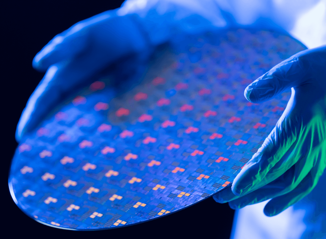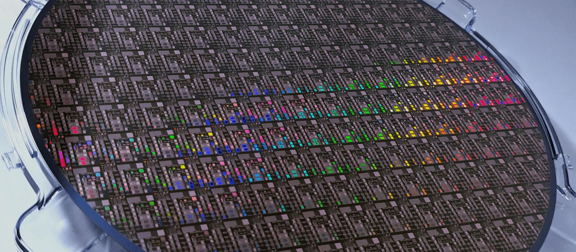
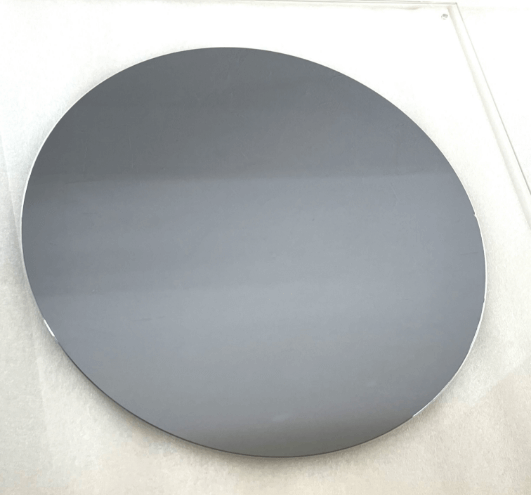
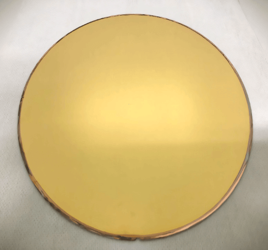
test wafers
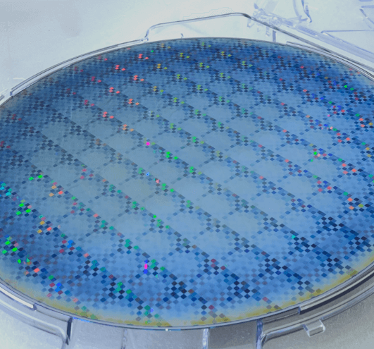
We supply a variety of bare, blanket, and patterned wafers to meet a wide range of research and development needs.
We are pleased to support various wafer diameters, film types, film thicknesses, and structures upon customer request.
Service
We have excellent suppliers in Japan and overseas, including the U.S., Europe, Korea, and Taiwan, and are well established to provide stable supply and high quality products.
Purchase Steps

Inquiry
We also accept inquiries through our website. Please feel free to contact us.


Quotation
We conduct careful discussions and propose products that put the customer’s needs first.

Ordering
We will follow up until delivery with full support.

Production
We manufacture custom-made wafers with our partner manufacturers with extensive experience.

Delivery
We deliver wafers safely and quickly.

WHAT IS
TEST WAFER?
Test wafers are wafers used to evaluate the equipment and materials needed to develop next-generation semiconductor processes. Semiconductor manufacturers are working to develop cutting-edge process technologies to enrich people’s lives. They are supported by material suppliers and semiconductor equipment manufacturers who conduct experiments and research every day to develop the next generation of state-of-the-art technologies.
In order to improve process uniformity on wafers, data collection using actual wafers is essential. We manufacture and supply test wafers for the development of next-generation semiconductors in the form of “custom-made” wafers that meet our customers’ requirements. Our products include wafers incorporating the latest technologies required for film deposition, CMP, cleaning, etching and TSV R&D.